


 8 and 16-bit MCUs are an invaluable tool for performing small, specialized tasks. The tasks aren’t necessarily complex, but they can be time consuming or time critical. By offloading the tasks, the 32-bit devices can have simpler implementations that improve reliability, reduce memory usage, and lower power consumption.
In today’s world, large 32-bit microcontrollers and microprocessors running a real time operation system (RTOS) are increasingly common. However, a single large microcontroller handling a complex application may run into issues with CPU resources with regards to small housekeeping tasks, which are not complex, but are time consuming.
Smaller devices, like 8 and 16-bit MCUs, can be used to offload these tasks from the 32-bit device. Consider the following example: a 32-bit MCU is used to control the non-safety features of a car, like the entertainment system, ambient lighting, and the A/C. The 32-bit device must allocate its resources to process all of the tasks associated with these features. A few examples include measuring the temperature of the cabin in multiple points, turning on/off the A/C systems, updating the graphical display, processing user inputs, adjusting lighting conditions, and playing music. Even for a large 32-bit device, this is a lot of work.
However, these tasks are more manageable if the 32-bit device offloads some of these tasks to sub processors that handle only 1 or 2 of these tasks but require little supervision in doing so. This frees up CPU resources on the main processor, which reduces software complexity while improving performance and execution time.
This solution is analogous to the benefits of peripherals in microcontrollers. Peripherals are small blocks of specialized hardware that can add new features (such as an operational amplifier or an analog-to-digital converter) or can reduce the amount of work the CPU must perform for a given function. In some cases, peripherals can run independently of the CPU after being initialized.
As an example, to show the benefit of peripherals, consider the generation of a Pulse-Width Modulated (PWM) signal. To generate PWM without a dedicated peripheral, simply set an I/O line HIGH, wait a certain number of cycles, set it LOW, wait some more, and repeat. This eats up a lot of CPU cycles and is difficult for something like an RTOS to execute reliably. A PWM peripheral, by contrast, lets the CPU set the desired waveform parameters while performing other tasks.
The first example provided shows the benefit of offloading a CPU intensive task. In this case, an 8-bit MCU is used to create an I/O expander. I/O expanders are not complex devices; however, they use a lot of CPU time due to the frequent servicing of interrupts. By using a dedicated MCU for just this task, the larger 32-bit device can reduce it is I/O utilization and the number of interrupts it needs to handle. Additionally, the I/O expander’s feature set is set in software, which allows it to be customized and tuned for the application.
The second example in this article shows the performance of core-independent peripherals to create a Voltage-to-Frequency (V/F) converter that operates independently of the CPU. The only functionality the CPU has in this example is to initialize the peripherals and to print debug messages to UART. In a larger system, the CPU could perform another simple task while the V/F ran in the background.
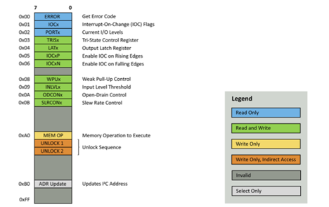
Figure 2 - Lookup Table of the Advanced I/O Expander.
I/O EXPANDER
The biggest benefit of creating an I/O expander using an 8-bit MCU is the flexibility. The feature set of an I/O expander ASIC is baked into the device, whereas the MCU defines its behavior based on the software it executes. This flexibility allows the MCU-based version to be adapted to fit the needs of the end application.
IMPLEMENTING THE ADVANCED I/O EXPANDER
Internally, the advanced I/O expander operates on a lookup-table based structure. Before reading or writing, a virtual address is sent. This address does not correlate with registers on the microcontroller – it is only specific to the lookup table. This means that features not in the hardware registers of the microcontroller can be added transparently. Entries in the table can be easily rearranged for specific uses as well. Another benefit of this structure is the ability to add permissions to the lookup table. For instance, to create a read-only register, simply omit the write lookup table entry.
This more complex structure also lends itself to non-standard functionalities. The function “MEM OP” allows the MCU to save or load its current General-Purpose Input and Output (GPIO) configuration to memory.
MEM OP can also reset the GPIO configuration to the parameters set when compiling.
Optionally, the microcontroller can be set to load the saved settings on power-up. If enabled, the microcontroller attempts to load the settings in configuration 0. If the configuration fails checksum validation, then the MCU will revert to the compile time constants. This feature can be disabled in the software, if not desired.
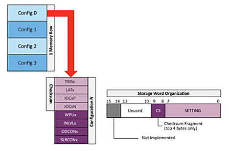
Figure 3 - Functionality of MEM OP.
TAKEAWAYS FROM THIS SOLUTION
The advantage of the MCU based solution is in the extreme amount of flexibility. Unlike the ASICs on the market, the MCU can be configured with non-standard functionalities specific to the application in use. This application was developed for the general-purpose PIC16F15244 family of MCUs.
For more information about the implementation or to try out the example, please see the README files in the source repositories. Demonstrations of the advanced I/O expander with an Arduino are also available.
Source Code, Documentation, and Demonstrations: https://github.com/microchip-pic-avr-examples/pic16f15244-family-advanced-i2c-io-expander
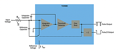
Figure 4 - Application Schematic for the TC9400/TC9401/TC9402 10 Hz to 100 kHz V/F Converter.
VOLTAGE-TO-FREQUENCYã´(V/F) CONVERTER
The voltage-to-frequency converter improves upon the traditional analog solution by reducing the Bill of Materials (BOM) and thus the design area. Many of the V/F converters on the market require external resistors and capacitors to operate, whereas the microcontroller only requires generic decoupling and pull-up components (required by all MCUs) to function.
Rather than using analog techniques to digitize, the MCU uses a combination of core-independent peripherals and features. The MCU measures the input signal with the internal Analog-to-Digital Converter with Computation (ADCC) then divides a clock signal to create a variable frequency output. In this example, the peripherals have been setup to operate autonomously of the CPU after initialization. This means the CPU could be used for other tasks in the end-application.
One challenge with the MCU based approach is that it does not perform as well as the analog solution does. The resolution of the output is intrinsically limited by the ADCC. Nominally, the ADCC is 12-bits, but with the way the program is configured, the ADCC runs at an oversampled 14-bit resolution. Likewise, the on-board Numerically Controlled Oscillator (NCO) that synthesizes the output frequency has finite resolution and can have jitter in its output, depending on the value measured by the ADC.
The MCU based solution can be split into three distinct blocks of peripherals – an analog sampling block, an output oscillator block, and a duty cycle generator.
ANALOG SAMPLING BLOCK
The analog sampling block is responsible for the analog-to-digital conversion. For an output of 100 kHz to be possible with the frequency limits of the device, the ADCC has been configured to oversample, then average down to get a 14-bit result.
A downside to this oversampling is the extra statistical noise added to the result. The noise is compensated for by averaging the oversample and adding hysteresis. To implement hysteresis, the threshold interrupt feature of the ADCC is used. (For simplicity, only the specifics of how this example uses the threshold interrupt feature will be covered.)
When the ADCC finishes computing the averaged oversample, the resulting value is compared to a setpoint register in the peripheral. If the difference between the two is greater than or less than set thresholds, then an interrupt is triggered. The CPU masks this interrupt and is unaffected, however this interrupt triggers a Direct Memory Access (DMA) copy of the averaged oversample result to the setpoint register of the ADCC, creating hysteresis. If the thresholds are not exceeded, then the DMA copy will not occur, which will not trigger the output oscillator block’s DMA to update.
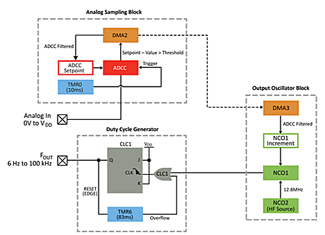
Figure 5 - Analog Sampling Block Implementation.
OUTPUT OSCILLATOR BLOCK
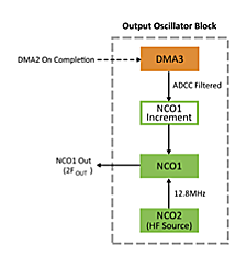 The output oscillator block (pictured left) of this solution is responsible for generating a clock signal at the desired output frequency. This output signal is internally connected to the duty cycle generator, which halves the frequency of the output but creates a 50% duty cycle output. Due to this, the output oscillator block runs at twice the frequency of the output.
The heart of the output oscillator block is a Numerically Controlled Oscillator (NCO). The NCO peripheral works by adding an increment value to an accumulator on the rising edge of an input clock. The accumulator overflow is used to derive the output of the peripheral. (For the full explanation on the NCO, please consult the datasheet.)
In this example, NCO2 has been setup to internally create the required input clock frequency to get a 100 kHz output from a 14-bit input. The 14-bit result is used because the native 12-bit result from the ADCC is not large enough to generate the 100 kHz output without an external clock source.
DUTY CYCLE GENERATOR
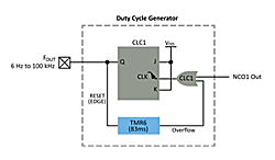 The Duty Cycle Generator block of this solution (pictured right) is responsible for the creation of a 50% duty cycle output. This feature is optional – the output from the NCO can be used directly, although the duty cycle will vary to a much larger degree.
This generator is implemented using one of the Configurable Logic Cells (CLC). The CLCs are small blocks of discrete configurable logic, similar to a single cell of an Field Programmable Gate Array (FPGA). CLCs can be used as discrete logic gates, such as AND-OR or OR-XOR. They can also be configured as latches or flip-flops. In this solution, a CLC was implemented as a J-K flip-flop with Reset. J and K are kept at logic HIGH.
The output oscillator block is used as the clock for the flip-flop. Every input clock pulse causes the output to toggle, which generates a 50% duty cycle. Note: frequency jitter from the output oscillator block will affect the duty cycle.
Timer 6 is used as an astable “watchdog” timer. If the output does not produce an edge (rising or falling), then the timer will overflow and generate a clock pulse to the CLC. This controls the low side of the output frequency range. Rather than reaching DC, the output toggles at the half of the frequency of the timer, for an output of 6 Hz.
TAKEAWAYS FROM THIS SOLUTION
This example demonstrates the use of hardware peripherals to create a core-independent function that ordinarily would have to be created with an external integrated circuit. One of the biggest benefits to this configuration is that the peripheral operation is setup in software, making it easy to adjust the example to the end-application. For implementing the example, the PIC18-Q43 family of MCUs was selected due to the large number of peripherals in use.
For more information about this example, please see the README document in the example repository. The example repository also contains an implementation of a frequency-to-voltage converter that can be implemented on the same device as the voltage-to-frequency converter.
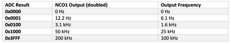
Table 1: Ideal Outputs of the 100kHz V/F Converter, with Watchdog Turned Off.
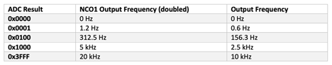
Table 2: Ideal Outputs of the 10kHz V/F Converter, with Watchdog Turned Off.
By Robert Perkel, Microchip Technology
Originally published in ETNdigi issue 2-2022


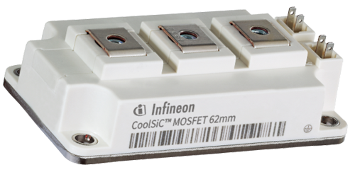
 IGBT on pitkään ollut teollisuuden tukipilari, joka yhdistää suuren tehon yksinkertaisiin ohjaustapoihin. Uuden polven IGBT7-teknologia on saanut merkittäviä parannuksia verrattuna aiempiin sukupolviin: alhaisempi myötäjännite, suuremmat nimellisvirrat, ylikuormituskapasiteetti 175°C asti, tarkempi dv/dt-säätö ja laadukkaampi suojadiodi.