


SiC vai GaN vai MOSFET vai IGBT:t? Jokaisella on oma paikkansa. Power Integrations uskoo galliumnitridiin teknologiana. Lopulta se valtaa markkinat aina satojen kilowattien teholuokkiin asti.
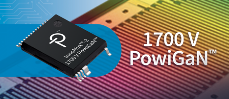
Käsitys GaN-teknologian asemasta on muuttunut merkittävästi uusimpien GaN-komponenttien julkaisun myötä. Power Integrations esitteli GaN-komponentin, jonka läpilyöntijännite on 1700 V. Tämä on 450 volttia aiempaa huippua enemmän ja 70 % enemmän kuin mitä mikään muu valmistaja tarjoaa.
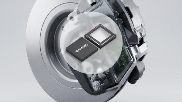
Suurin osa GaN-yrityksistä kamppailee päästäkseen edes 750 V yläpuolelle. PI on julkaissut flyback-tyyppisen tehonsyöttöpiirin, InnoMux-2:n, joka on luokiteltu 1700 V:iin, joten se soveltuu erinomaisesti esimerkiksi 1000 VDC -väyläjärjestelmiin. Tuote on tilattavissa 16 viikon toimitusajalla volyymituotantoon, ja näytteitä on heti saatavilla.
Mitä tämä tarkoittaa teollisuudelle ja koko "GaN vs. SiC – mikä on paras teho-IC-teknologia?" -keskustelulle? PI uskoo, että GaN tulee pian soveltumaan kaikkiin sovellussektoreihin aina matalista, kymmenien wattiin tehoista useisiin satoihin kilowatteihin saakka.
GaN on jo voittanut pienitehoisten laturien markkinan noin 30 W:sta 240 W:iin. Tämä johtuu siitä, että se on huomattavasti tehokkaampi kuin Super Junction MOSFETit, koska GaN:lla on käytännössä olemattomat kytkentähäviöt ja erittäin alhainen ominaisvastus (RDSON). Tämän ansiosta saavutetaan suurempi tehopakattu tiheys, laitteet voivat olla pienempiä tai tehokkaampia, ja lämmönhallinta on paljon helpompaa.
Vaikka MOSFETit ovat tällä hetkellä halvempia kuin GaN-HEMTit, niiden vaatimat kehittyneet resonanssitopologiat ja jäähdytyselementit tekevät niistä järjestelmätasolla kalliimpia kuin GaN. GaN:n etu vain kasvaa, kun mittakaavaedut alkavat vaikuttaa ja tuotanto kasvaa. Ainoa syy, miksi MOSFET saattaa olla parempi valinta hyvin matalatehoisissa sovelluksissa (esim. alle 20 W), on se, että GaN-sirut ovat niin pieniä tällä tehotasolla, että niiden käsittely on haastavaa.
Artikkeli löytyy kokonaisuudessaan alla ja uusimmasta ETNdigi-lehdestä.
GaN IS WINNING THE POWER BATTLE
SiC v GaN v SJ MOSFETs v IGBTs? Each has its place and that’s why we, at Power Integrations, do not treat GaN as a market, it’s a technology. It’s just one of many in our armoury, along with SiC and various different MOSFET technologies and we use what we determine to be the most appropriate, application by application.
Doug Bailey, Power Integrations
The perception of GaN’s place has changed significantly with our recent dramatic launch of a GaN device – and I think that is a justifiable adjective to use – with a breakdown voltage of 1700 V. Let’s put that into perspective: 1700 V is 450 V higher than our previous best, and 70% higher than the best offered by any other maker (which, incidentally, we believe is currently not available as a shippable high-volume product). Most GaN companies are struggling to get much above 750 V. We launched a flyback power supply IC, InnoMux-2, that is rated at 1700 V, so it can easily cope with 1000 VDC rail applications. It is available to order with a 16-week delivery lead time in volume, and samples are available off the shelf.
What does this mean for industry and the whole ‘GaN v SiC, which power IC technology is best’ discussion?
In short, we believe that GaN will soon be able to address all application sectors from the low 10s of watts up to 100s of kilowatts.
Let’s break it down. GaN has already won the low power charger market from 30 W to, say, 240 W. This is because it is much more efficient than Super junction MOSFETs, featuring negligible switching losses and very low specific RDSON. Therefore, higher power densities are achievable, devices can be made smaller or more powerful, and the thermal management challenge is much reduced. Although MOSFETs are currently cheaper than GaN HEMTs, the need for advanced resonant topologies and heatsinks makes them less cost-effective than GaN at the system level. This GaN advantage will only improve as economies of scale kick in and production ramps up. The only reason why MOSFETs may be preferred for very low power applications (for example <20 W) is that the GaN die at low power levels are so small they are hard to handle.
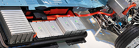
As we move up in power levels through 500 W, 1 kW and up to 10kW, GaN is also winning. Here we are looking at applications such as refrigerators, e-bike chargers, washing machines and other white goods, HVAC compressors, solar, certain automotive functions such as the on-board charger and lead-acid replacement battery circuits, and server PSUs. All these are transitioning from MOSFETs. Some have already made the move to SiC, and since SiC and GaN have comparable efficiency ratings, why should GaN prevail here? Simply, the reason is cost. SiC requires huge amounts of energy to create the high processing temperatures required. GaN does not. A GaN device is inherently no more expensive to produce than a silicon part – devices can even be made on the same production lines with relatively few modifications.
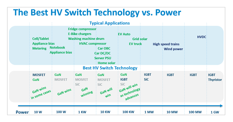
Kuva 1. GaN has already won the low power charger market from 30 W to 240 W.
More and more of these 1 to 10kW applications – previously the preserve of MOSFETs and SiC - will be addressable by GaN, and it won’t stop there. Currently, GaN tops out at around 7-10 kW. That’s a little short of satisfying the needs of the EV inverter market – the biggest single power IC application TAM – but you only need another factor of 10 to get to EV power levels of a few hundred kW, and a factor of 10 in high tech is a matter of just a few years. There's no substantive constraint, there's no physical limitation…it’s not invention or inspiration that is needed, it's development.
At the very high power end of the scale - multi-megawatt wind turbines and gigawatt high-voltage DC installations - IGBTs are well established and comparatively cheap. Therefore, SiC looks set to be squeezed into a relatively small section of the market, which needs the higher currents that the vertical technology can offer.
One final point. When any new technology comes along, or takes a significant step forward, the first thing it does it to directly replace the previous tech. But then someone bright comes along and says, ‘well that’s OK, but the new tech allows us to completely rethink the design – to come up with a new concept that makes best use of the new technology without referring back to what was required by the old’. We’re continuing to innovate at the microelectronics, packaging, system, and algorithm levels to develop application-specific power products that advance efficiency, cost-effectiveness, and component count, opening up new ideas for new markets.
 Tekoäly siirtyy pilvestä koneisiin, kameroihin, antureihin ja robotteihin. Reunalla yksi laitteistoratkaisu ei kuitenkaan sovi kaikkeen, vaan suorituskyky on sovitettava mallin, datan ja käyttökohteen mukaan.