Sulautettuja järjestelmiä on kehitetty vuosikymmeniä. Hiljattain esineiden internet eli IoT, joka kattaa useimmat sovellusalueet, on saanut aikaan kehitysvuon ja tekniikoiden renessanssin, joka pyrkii tuomaan järjestelmät markkinoille nopeammin. Nopeuden lisäksi vanhojen moottoreiden eli suorituskyvyn, tehonkulutuksen ja kustannusten rinnalle on IoT-aikana tullut turvallisuus, liitettävyys ja päivitettävyys kentällä.
| Cadence Design Systemsin System and Verification -ryhmän tuotteiden hallinnasta vastaava johtaja Frank Schirrmeister on kirjoittanut artikkelin, jossa lääkkeeksi näihin vaatimuksiin esitetään integroitua verifioinnin, emuloinnin ja FPGA-pohjaisen prototypoinnin alustaa. |
Embedded System Development has been around for decades. Recently the Internet of Things (IoT), spanning across most application domains, has contributing to a renaissance of development flows and techniques to bring embedded systems to market fastest. Besides time to market, in the past considerations for performance, power and cost were key development drivers, in the age of IoT they are now joined by other priorities like security, connectivity and in-field upgradeability.
Integrated verification, smartly combining formal verification, simulation at the transaction and classic register transfer level (RTL), emulation and FPGA based prototyping has become a key requirements. Given the varying development needs for edge nodes, hubs, networks and servers, trying to meet varying priorities across multiple application domains, the vehicles for verification and software development need to be extremely flexible and require close interaction. Figure 1 shows the Cadence Verification Suite with its four corer engines formal, simulation, emulation and prototyping.
It is crucial for development teams to be able to efficiently move a design through the different engines, and to capitalize on the individual strength of the engines by optimally combining them. A verification fabric spans across the engines and provides a unified user experience for key tasks like verification management, debug and portable testing. In combination, engines and fabric are geared to optimize total throughput for designs, allowing fastest time to market and to allow metric driven design giving developers clear indication when they are ready to proceed and roll out their products.
The resulting software development and verification flows are optimized for specific application domains, for example adding specific capabilities around functional safety and ISO 26262 compliance for automotive, and are architected to be remotely accessible through cloud based design.
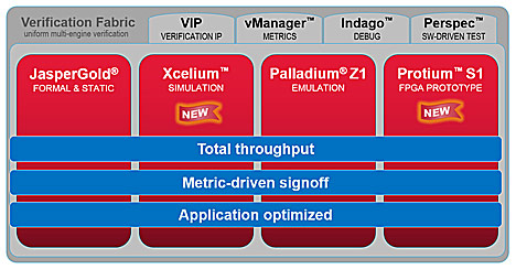
Figure 1 – The Cadence Verification Suite
Emulation and FPGA based prototyping have long been available to accelerate speeds, extending the range of verification into hardware/software verification, software development and system validation. In the era of IoT, embedded software development clearly has become the long pole in the tent, gating time to product delivery and with that time to revenue. While Emulation is based on its availability often used for lower level software development, it has always been somewhat speed limited. In contrast FPGA based prototyping generally achieves the appropriate performance that satisfies the needs of software developers. However, time to prototype, due to the largely manual optimizations required and the need to re-write the RTL to make it FPGA friendly, has traditionally been long, often taking months, depending on the size of the hardware portion of the embedded system.
Cadence Protium S1, together with the Cadence Palladium Z1 Enterprise Emulation Platform, directly addresses these challenges and revolutionizes bring-up time by an average of 80% from months to weeks or even days. It gives users the fastest path to prototype for software development, system validation and hardware regressions. Depending on the size of the hardware, Protium S1 comes in different configurations from Protium S1-G single FPGA boards for designs up to 25 million gates to Protium S1 multi chassis combinations of up to 6 boards that can prototype up to 600 million gates.
One key challenge for FPGA based prototyping of embedded systems is modeling of memories. ASIC memories are usually very different from the FPGA-internal memories as they typically more than 2 ports and have different WRITE_ENABLE characteristics. Therefore, to make this work in the FPGA environment, users need to add multiplexers to implement a multi-port behavior and WRITE_ENABLE circuitry to make sure that the write access occurs at the correct time and in sync with valid address and data. Modeling all design memories manually can be a long and cumbersome process. With Protium S1, memory modeling is done quickly and automatically, as shown in Figure 2. The clock generation logic is replicated in every FPGA, while the reset logic is implemented in one FPGA only, which in fact, can be any of the FPGAs. The reset logic is needed to synchronize the clocks across the multiple FPGAs.
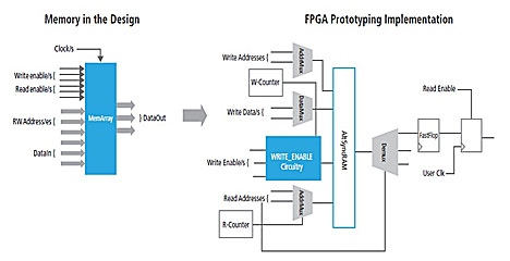
Figure 2 – Memory Modeling in Protium S1
Another challenge for FPGA based prototyping is clock distribution across multiple FPGAs as well as clock synchronization. When a design is partitioned into multiple FPGAs, primary clocks required for the design have to be driven to the FPGAs. These clocks need to have tight phase relationship between the FPGAs. Designs typically have 10s of primary clocks with a wide range of frequency requirements. Having that many clock sources on the board and distributing them to all the FPGAs is not an efficient solution. To address that, the Protium S1 compile flow automates clocking and uses the built-in PLLs in the FPGAs to generate these clocks locally. This requires only one global clock to be routed to all the FPGAs. The PLLs can use this clock as the reference clock the clocks across FPGAs are synchronized with a common reset signal.
In addition, Protium S1 used automated cycle based clocking for the fully automated flow as shown in Figure 3. The compiler automatically generates a conceptual clock called FCLK to which all the clocks in the design are synchronized and all the nets in the design are updates once per FCLK cycle. Using this technology – similar to what is used on processor based emulation - a unlimited # of design clocks are supported, hold-time violations are completely avoided, FPGA-specific clock limitations are removed and FPGA timing closure and FPGA place and route time are improved.

Figure 3 – Clock Synchronization in Protium S1
But that’s not where performance stops. Protium S1 is scalable from 3MHz to 100MHz, from fully automatic to fully manual. Protium S1’s automated front-end allows further optimization of clocking, critical paths and memory ports. Together with higher effort place and route this extends the speed range easily to 10 MHz. To extend performance even further, the Protium S1 hardware can replace home grown FPGA systems easily and allows with manual optimization to get to 10’s of MHz performance.
For embedded software development, Protium S1 offers very specific, unique capabilities not found in any other FPGA based prototyping systems. Memory upload and download together with capabilities to freely start and stop the design, force and release signals enable advanced software debug. Protium S1 also has a transaction interface that allows host based software to be connected.
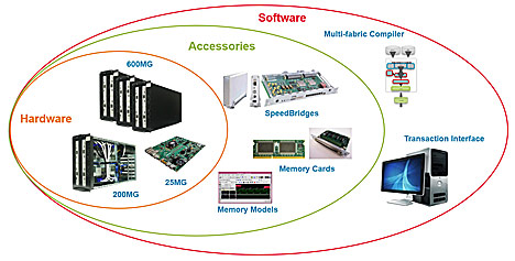
Figure 4 – Cadence FPGA Based Prototyping Portfolio
In addition to being equipped with a variety of on-board interfaces, the Protium S1 Platform is complemented by a comprehensive portfolio of daughter cards. The Protium S1 Platform is also fully compatible with Cadence’s family of SpeedBridge adapters, enabling a smooth transition from an emulation environment to a FPGA-based prototyping environment.
The resulting FPGA based prototyping portfolio is shown in Figure 4. As part of the industry leading Cadence Verification Suite, FPGA Based Prototyping for embedded systems has just become a lot easier with Protium S1.






 – Haluamme olla tekoälyn hyödyntämisen edelläkävijöitä, ja se vaatii luottamuksen rakentamista asiakkaiden suuntaan. Pelkkä yrityksen oma lupaus ei enää riitä, sanoo Julius Manni. Vincit on saanut ensimmäisenä Suomessa akkreditoidun ISO/IEC 42001 -sertifikaatin.

